
Quick Summary: Machine learning is revolutionizing the semiconductor industry by optimizing manufacturing processes, improving defect detection, and enhancing yield management. From predicting equipment failures to streamlining chip design, ML technologies are addressing the complex challenges of semiconductor fabrication. As of 2026, leading manufacturers are deploying AI-driven solutions that reduce production costs, accelerate time-to-market, and enable data-driven decision-making across the entire semiconductor value chain. Semiconductor manufacturing is one of the most demanding industries on the planet. Each chip requires hundreds of intricate steps, with thousands of parameters that can impact performance, reliability, and yield. And here’s the thing—traditional quality control methods simply can’t keep up anymore. The complexity has exploded. Machine learning has emerged as the critical technology solving these challenges. But it’s not just hype—real implementations are delivering measurable results across fabrication facilities worldwide.
The Manufacturing Challenge That ML Solves
Semiconductor production generates massive amounts of data. Every wafer, every process step, every piece of equipment creates information that was historically underutilized. Manual inspection by human experts typically achieves defect detection rates of 60-80%, according to research on multi-project wafer manufacturing. That’s a significant quality gap when dealing with high-value products. ML algorithms can process this data at scale, identifying patterns invisible to human observation. In practice, these systems operate continuously without fatigue, analyzing optical profilometry data, process parameters, and equipment sensor readings in real-time. 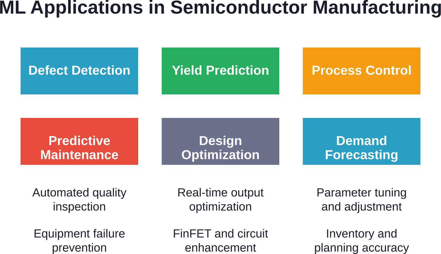
Defect Detection: Where ML Shows Immediate Value
Optical profilometry combined with machine learning models has demonstrated impressive capabilities. Research using optical profilometry shows that ML can predict low voltage properties of vertical GaN diodes with over 75% accuracy. That’s a substantial improvement over manual methods. But wait—there’s more. The technology excels at identifying defects that reduce breakdown voltage in gallium nitride (GaN) devices. These substrates are crucial for high-voltage and high-frequency power applications, where manufacturing defects can prevent vertical devices from achieving optimal performance. Deep learning models have proven particularly effective for defect identification tasks. Training approaches incorporate both real and synthetic wafer datasets to develop robust detection capabilities across various defect types and conditions. The National Institute of Standards and Technology documented the importance of open and scaled data sharing for advancing AI applications in semiconductor manufacturing in their workshop report (published 2025-11-18). Data accessibility remains a key enabler for ML progress.
Real Production Impact
Leading semiconductor manufacturers are reporting tangible benefits. According to industry analysis, long-range forecast accuracy at leading semiconductor firms had stagnated around 70% for years using traditional methods. The analysis revealed something striking: each additional percentage point of forecast accuracy would reduce one full day of inventory. In an industry where working capital efficiency directly impacts competitiveness, that matters enormously.
| Detection Method | Accuracy Rate | Speed | Consistency |
|---|---|---|---|
| Manual Inspection | 60-80% | Slow | Variable |
| ML-Based Systems | 75%+ | Real-time | Continuous |
| Hybrid Quantum-Classical | Under Research | High Potential | Experimental |
Process Optimization and Design Enhancement
Machine learning algorithms are transforming how engineers optimize semiconductor processes. IEEE research has documented ML applications in FinFET transistor design optimization for energy-efficient computing, flip chip package structural design, and spiral inductor optimization on LCP substrates. These aren’t theoretical exercises. The models enable faster iteration cycles, exploring design spaces that would be impractical through traditional simulation methods. Process parameter optimization benefits from ML’s ability to identify non-obvious relationships between variables. Temperature profiles, deposition rates, etching durations, and chemical concentrations all interact in complex ways that resist simple analytical solutions.
Yield Management and Predictive Maintenance
Yield optimization represents one of the highest-value ML applications. Small improvements in yield translate directly to profitability in an industry where margins depend on extracting maximum value from each wafer. ML models analyze historical production data to identify process conditions correlated with higher yields. These insights guide adjustments to recipes, equipment settings, and material selections. Predictive maintenance algorithms monitor equipment health in real-time, detecting early warning signs of degradation or failure. The semiconductor industry operates some of the most expensive manufacturing equipment in existence—unplanned downtime costs are substantial. NIST has established integrated CMOS testbeds specifically for developing nanoelectronics and machine learning accelerator technologies. These testbeds enable researchers to explore novel nanodevices, circuit architectures, and functionalities for next-generation computing architectures.
The Data Challenge
Here’s the reality though: effective ML requires substantial high-quality training data. Semiconductor manufacturers have historically been protective of process data due to competitive concerns. The NSF-sponsored workshop on artificial intelligence with open and scaled data sharing addresses this limitation. Collaborative frameworks that enable data sharing while protecting proprietary information could accelerate ML advancement across the industry. Data preprocessing remains critical. Raw sensor outputs require cleaning, normalization, and feature engineering before feeding into models. Domain expertise guides this transformation—ML augments rather than replaces engineering knowledge.

Boost Your Production Yield with Ph.D.-Level AI
Precision manufacturing requires scientific rigor and custom machine learning models. AI Superior develops end-to-end AI solutions, leveraging a team of Ph.D. data scientists to solve complex production bottlenecks.
Want to Automate Quality Control and Minimize Downtime?
AI Superior provides specialized AI development to optimize your fab operations:
- Computer vision systems for high-speed defect detection and image analysis
- Predictive models to forecast equipment failures and prevent costly downtime
- Big Data analytics to identify actionable patterns in your manufacturing data
👉Contact AI Superior today to discuss your technical requirements and get a project estimate.
Emerging Applications and Future Directions
Quantum-classical hybrid deep learning approaches are under investigation for semiconductor defect detection. These experimental systems combine quantum computing elements with conventional neural networks, potentially offering computational advantages for specific pattern recognition tasks. The technology remains in research phases but demonstrates the ongoing innovation in ML methodologies applied to semiconductor challenges. Design automation tools increasingly incorporate ML components. These systems can suggest layout optimizations, predict electrical characteristics from structural designs, and accelerate verification processes. Supply chain applications are expanding as well. Demand forecasting, inventory optimization, and logistics planning benefit from ML’s ability to identify complex patterns in market dynamics and consumption trends.
FAQ
How accurate is machine learning for semiconductor defect detection?
ML models have demonstrated over 75% accuracy in predicting specific properties of vertical GaN diodes; they currently match or complement the 60-80% accuracy range of manual inspection.
What types of semiconductor manufacturing processes benefit most from ML?
Defect detection, yield prediction, process control, predictive maintenance, and design optimization show the strongest benefits. Applications involving large datasets, complex parameter relationships, or real-time decision requirements are particularly well-suited to ML approaches.
Do manufacturers need specialized equipment to implement ML solutions?
Not necessarily. Many ML systems work with existing sensor data and metrology equipment like optical profilometers. Integration with standard manufacturing execution systems enables deployment without major capital investments, though data infrastructure upgrades may be required.
How does ML compare to traditional statistical process control?
ML excels at identifying non-linear relationships and high-dimensional patterns that traditional statistical methods struggle with. However, ML complements rather than replaces conventional approaches—many facilities use hybrid systems combining both methodologies for optimal results.
What data volumes are required to train effective ML models?
Requirements vary significantly by application. Simple classification tasks may need thousands of labeled examples, while complex deep learning models can require millions. Transfer learning and synthetic data generation techniques help reduce data requirements in some scenarios.
Can small semiconductor manufacturers benefit from ML?
Absolutely. Cloud-based ML platforms and pre-trained models lower barriers to entry. Collaborative research initiatives and shared datasets enable smaller operations to access advanced capabilities without building infrastructure from scratch.
What are the main challenges in deploying ML for semiconductor manufacturing?
Data quality and availability, model interpretability, integration with legacy systems, and workforce training represent the primary obstacles. Competitive concerns around data sharing and the need for domain expertise to guide implementation also present challenges.
Conclusion
Machine learning has moved beyond experimental phases in the semiconductor industry. Real implementations are delivering measurable improvements in defect detection, yield management, process control, and operational efficiency. The technology addresses fundamental challenges that traditional methods struggle to solve—managing complexity, processing massive data volumes, and optimizing multi-variable systems in real-time. Success requires careful attention to data quality, thoughtful model selection, and integration of domain expertise. ML tools augment human capabilities rather than replacing engineering judgment. Organizations exploring ML deployment should start with focused pilot projects in high-value areas like defect detection or predictive maintenance. Build data infrastructure deliberately, establish clear success metrics, and scale proven solutions systematically. The semiconductor industry’s future competitiveness increasingly depends on effective AI and ML adoption. Companies that master these technologies will have significant advantages in yield, quality, and time-to-market.