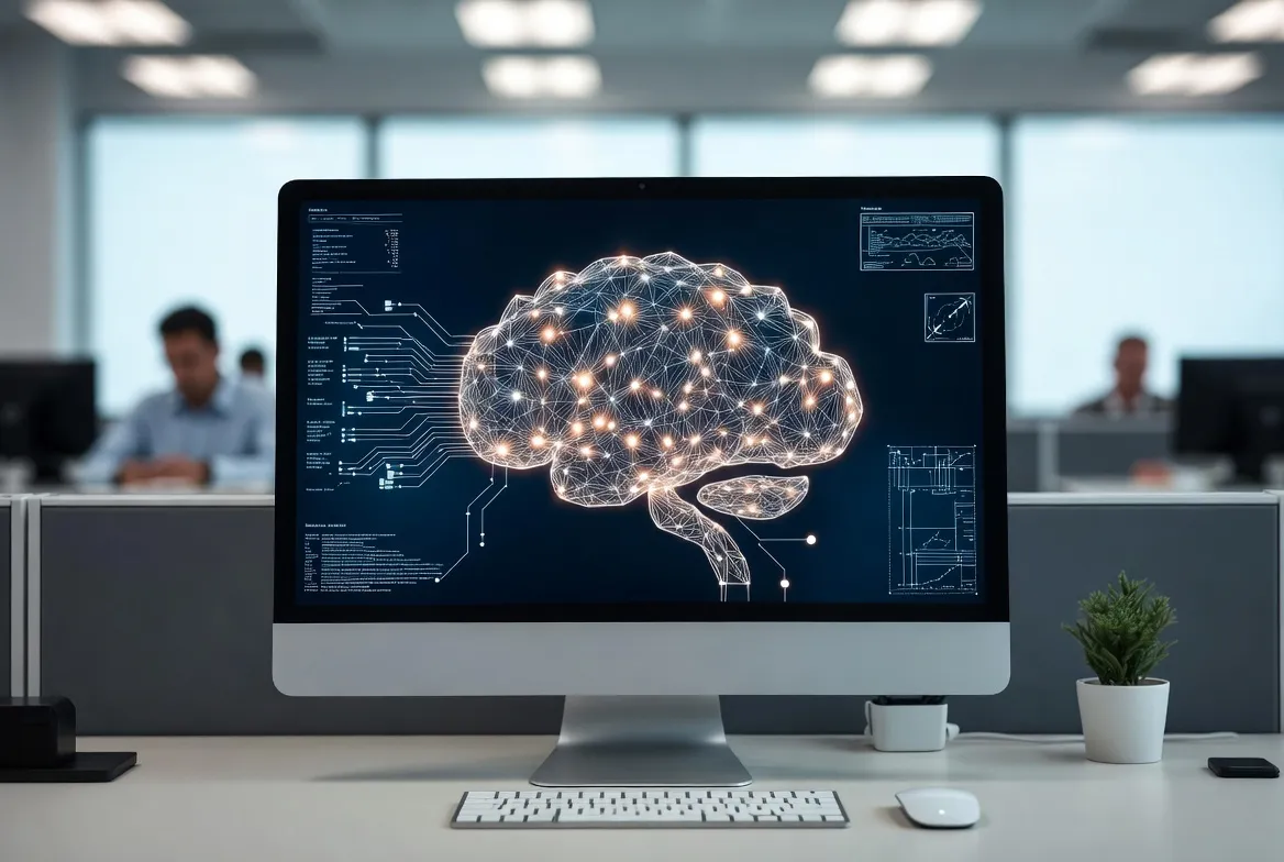
Kurzzusammenfassung: Maschinelles Lernen revolutioniert das Chipdesign durch die Automatisierung traditionell manueller Aufgaben wie Floorplanning, Routing und Verifikation. ML-Algorithmen optimieren Layouts, prognostizieren den Stromverbrauch, verkürzen Entwicklungszyklen von Monaten auf Wochen und ermöglichen spezialisierte Architekturen für KI-Workloads, während gleichzeitig Speicherbeschränkungen auf Edge-Geräten berücksichtigt werden.
Die Halbleiterindustrie steht vor einem Paradoxon. Chips müssen mit jeder Generation schneller, kleiner und energieeffizienter werden – doch traditionelle Designmethoden können mit diesen Anforderungen nicht Schritt halten.
Hier kommt maschinelles Lernen ins Spiel. ML-Algorithmen übernehmen heute Aufgaben, für die früher ganze Ingenieurteams monatelang arbeiten mussten. Sie optimieren die Transistorplatzierung, sagen thermische Hotspots voraus und generieren Layouts, die menschliche Designer sich schlichtweg nicht hätten vorstellen können.
Aber wie genau funktioniert das? Und was bedeutet das für die Zukunft des Rechnens?
Warum das traditionelle Chipdesign an seine Grenzen stieß
Die Entwicklung moderner Halbleiter ist von enormer Komplexität. Ein einzelner Chip kann zig Milliarden Transistoren enthalten, von denen jeder eine präzise Platzierung und Verbindung erfordert.
Herkömmliche Werkzeuge zur elektronischen Entwurfsautomatisierung basieren stark auf Heuristiken – fundierten Annahmen, die zwar recht gut funktionieren, aber selten optimale Ergebnisse liefern. Ingenieure durchlaufen unzählige Entwurfsvarianten und führen Simulationen durch, deren Abschluss Wochen dauern kann.
Das Problem verschärft sich mit der Miniaturisierung der Chips. Bei Strukturgrößen ab 3 nm spielen Quanteneffekte eine bedeutende Rolle. Stromversorgungsnetze erfordern eine sorgfältige Planung. Das Wärmemanagement bedarf ausgefeilter Modellierung.
Die Designteams wachsen nicht proportional. Branchenanalysen zufolge steigt die Komplexität der Chips zwar exponentiell an, die Anzahl der Ingenieure bleibt jedoch relativ konstant.
Irgendwas musste nachgeben.
Wie maschinelles Lernen den Designprozess verändert
Maschinelles Lernen greift die Chipentwicklung gleichzeitig aus mehreren Blickwinkeln an. Anstatt menschliches Fachwissen vollständig zu ersetzen, erweitert ML die Fähigkeiten der Entwickler an kritischen Engpässen.
Automatisierte Grundrissplanung und Layout
Die Flächenplanung – die Festlegung der Position wichtiger Funktionsblöcke auf einem Chip – beanspruchte traditionell wochenlange Expertenarbeit. Ingenieure mussten dabei widersprüchliche Anforderungen abwägen: Minimierung der Drahtlänge, Optimierung der Wärmeableitung und Sicherstellung der Signalintegrität.
Reinforcement-Learning-Algorithmen generieren mittlerweile übermenschliche Grundrisse. Diese Systeme lernen aus Tausenden von Designiterationen und entdecken dabei nicht offensichtliche Optimierungen, die der menschlichen Intuition entgehen.
Die so entstandenen Layouts sehen oft unkonventionell aus. Aber sie funktionieren – und werden heute in weltweit eingesetzter Hardware verwendet.
Leistungs- und Performancevorhersage
Die Vorhersage des Verhaltens eines Designs vor der Fertigung ist entscheidend. Traditionelle Simulationsverfahren sind zwar genau, aber quälend langsam.
Auf Basis vorheriger Designs trainierte ML-Modelle können Stromverbrauch, Taktfrequenz und thermisches Verhalten um Größenordnungen schneller vorhersagen. Anstatt tagelang auf Simulationsergebnisse zu warten, erhalten Entwickler Schätzungen innerhalb von Minuten.
Dies ermöglicht eine schnelle Erkundung des Gestaltungsraums. Teams können Hunderte von architektonischen Varianten bewerten, deren Simulation mit herkömmlichen Methoden praktisch unmöglich gewesen wäre.
Verifizierung und Fehlererkennung
Die Verifizierung – die Sicherstellung der korrekten Funktion eines Chips vor der Fertigung – macht bis zu 701.030 Billionen Pfund Entwicklungsaufwand aus. Fehler, die dabei durchrutschen, verursachen nach der Fertigung Kosten in Millionenhöhe für deren Behebung.
Maschinelles Lernen zeichnet sich durch seine Mustererkennung aus. Trainiert mit Datenbanken bekannter Konstruktionsfehler, erkennen ML-Systeme verdächtige Schaltungsmuster, die auf Fehler hinweisen könnten.
Aktive Lernverfahren ermöglichen es diesen Systemen, sich kontinuierlich zu verbessern, indem sie aus jedem neu entdeckten Fehler lernen.

ML-Tools mit AI Superior entwickeln
AI Superior Das Unternehmen entwickelt KI- und Machine-Learning-Lösungen für Prognosen, Datenanalyse, Business Intelligence, Big-Data-Analysen, Computer Vision und kundenspezifische Softwareentwicklung. Die prädiktive Analytik nutzt aktuelle und historische Daten, um Vorhersagen zu treffen und fundiertere technische Entscheidungen zu ermöglichen.
Für Chip-Designteams kann dies die Analyse von Simulationsdaten, die Vorhersage von Fehlern, die Überprüfung von Designs, die Prozessoptimierung oder interne Tools unterstützen, die mit komplexen technischen Datensätzen arbeiten.
Benötigen Sie KI-Integration in Ihre Entwicklungsprozesse?
AI Superior kann Ihnen helfen bei:
- Erstellung von Modellen für maschinelles Lernen
- Entwicklung von Datenanalyse- und Prognosetools
- Testen von KI-Ideen durch PoC- oder MVP-Arbeit
- Verbindung von KI-Tools mit bestehenden Plattformen
👉 Kontaktieren Sie AI Superior um Ihr Projekt zu besprechen.
Spezialisierte ML-Architekturen für KI-Workloads
Hier wird die Sache rekursiv: Maschinelles Lernen bedeutet, Chips zu entwickeln, die speziell für maschinelles Lernen optimiert sind.
Herkömmliche CPUs waren nicht für die parallelen Matrixoperationen ausgelegt, die neuronale Netze erfordern. GPUs halfen zwar, sind aber universelle Parallelprozessoren mit eigenen Einschränkungen.
KI-spezifische Chips – TPUs, NPUs und kundenspezifische Beschleuniger – erfordern grundlegend andere Architekturentscheidungen als herkömmliche Prozessoren. Die Datenflussmuster unterscheiden sich. Speicherhierarchien müssen überdacht werden. Stromversorgungsnetze stehen vor besonderen Herausforderungen.
ML-gestützte Designwerkzeuge können diese neuartigen Architekturen effektiver gemeinsam optimieren als traditionelle Methoden. Sie erforschen unkonventionelle Designs, die menschliche Ingenieure möglicherweise als unpraktisch ablehnen würden.
Photonische Prozessoren durchbrechen Geschwindigkeitsgrenzen
Forscher am MIT haben einen photonischen Prozessor entwickelt, der neuronale Netzwerkberechnungen mit Licht statt mit Elektrizität durchführt und so ein schnelleres und energieeffizienteres Deep Learning ermöglicht.
Photonisches Rechnen beseitigt elektrische Engpässe vollständig. Signale breiten sich mit Lichtgeschwindigkeit durch optische Wellenleiter aus. Der Energieverbrauch sinkt drastisch, da photonische Operationen im Vergleich zum Schalten von Transistoren nur minimal Energie benötigen.
Die Entwicklung dieser Systeme erfordert völlig neue Methoden. ML-Algorithmen optimieren Wellenleitergeometrien, Gitterkopplerkonfigurationen und Phasenmodulatoranordnungen – Parameter, für die es kein elektrisches Schaltungsanalogon gibt.
TinyML: Maschinelles Lernen auf ressourcenbeschränkten Geräten
Nicht alle ML-Chips sind massive Rechenzentrumsbeschleuniger. TinyML ermöglicht neuronale Netzwerkinferenz auf Geräten im Wert von $1-$2 – Sensoren, Wearables und IoT-Endpunkte.
Die Herausforderung? Laut einer MIT-Studie aus dem Jahr 2021 stoßen diese Geräte bei Inferenzoperationen an ihre Speichergrenzen. Herkömmliche neuronale Netze sind dafür schlichtweg ungeeignet.
Patchbasierte Inferenz löst Speicherbeschränkungen
Forscher haben ein Verfahren entwickelt, das jeweils nur 25% der Feature-Map einer Ebene verarbeitet. Anstatt ganze Ebenen in den Speicher zu laden, verarbeitet die patchbasierte Inferenz die Daten in kleineren Blöcken.
Dieser Ansatz ermöglicht eine 4- bis 12-fache Speichereinsparung im Vergleich zur herkömmlichen schichtweisen Berechnung. Plötzlich laufen hochentwickelte Computer-Vision-Modelle auf Chips mit nur wenigen Kilobytes RAM – Geräte, die man mit einer Uhrenbatterie betreiben könnte.
Der Designprozess für TinyML-Chips erfordert die gemeinsame Optimierung von Hardwarearchitektur und ML-Modellstruktur. Automatisierte Tools durchsuchen diesen kombinierten Designraum und finden Konfigurationen, die die Genauigkeit innerhalb strenger Speicher- und Leistungsbudgets maximieren.
| Designaspekt | Traditioneller Ansatz | ML-gestützter Ansatz | Verbesserung |
|---|---|---|---|
| Grundrissplanung | Manuelle Iteration | Bestärkendes Lernen | 50-70% schneller |
| Leistungsabschätzung | Detaillierte Simulation | Trainierte Vorhersagemodelle | 10- bis 100-fache Beschleunigung |
| Überprüfungsabdeckung | Gezielte/zufällige Tests | Anleitung zum aktiven Lernen | 30-45% weitere Fehler gefunden |
| Erkundung des Gestaltungsraums | Begrenzte Proben | Schnelle ML-basierte Vorhersage | 100- bis 1000-mal mehr Optionen bewertet |
Maschinelles Lernen im Analog- und Mixed-Signal-Design
Die meisten Aufmerksamkeit gilt dem Design digitaler Chips, doch analoge Schaltungen bieten ebenso überzeugende Möglichkeiten für maschinelles Lernen.
Analog-Digital-Wandler veranschaulichen diese Herausforderung. AD-Wandler müssen Auflösung, Geschwindigkeit, Stromverbrauch und Linearität in Einklang bringen – Parameter mit komplexen, nichtlinearen Wechselwirkungen.
Untersuchungen haben gezeigt, dass ML-optimierte ADCs eine bis zu 40% höhere Energieeffizienz und ein um 3-5 dB verbessertes Signal-Rausch-Verhältnis im Vergleich zu herkömmlichen Architekturen erreichen.
Maschinelle Lernalgorithmen optimieren Transistorgrößen, Biasströme und Kompensationsnetzwerke gleichzeitig. Sie ermitteln Designpunkte in hochdimensionalen Parameterräumen, für deren manuelle Iteration menschliche Ingenieure Monate benötigen würden.
FinFET- und fortgeschrittene Knotenoptimierung
Bei modernsten Fertigungsprozessen wird die Bauelementphysik extrem komplex. FinFET-Transistoren verhalten sich anders als planare Bauelemente. Gate-All-Around-FETs führen zu noch mehr Variablen.
IEEE-Veröffentlichungen dokumentieren die ML-basierte Optimierung von FinFET-Transistoren für energieeffizientes Rechnen. Diese Algorithmen berücksichtigen Quanteneffekte, Prozessschwankungen und Temperaturabhängigkeiten, die mit herkömmlichen, auf Eckpunkten basierenden Designansätzen nur unzureichend erfasst werden.
Das Ergebnis? Chips, die die Leistungsziele erreichen, dabei weniger Strom verbrauchen und eine bessere Toleranz gegenüber Fertigungsschwankungen aufweisen.
Praxiseinsatz und Branchenakzeptanz
Das sind keine theoretischen Verbesserungen. Große Halbleiterunternehmen und Auftragsfertiger haben ML-gestützte Designwerkzeuge in Produktionsabläufe integriert.
Anbieter von EDA-Lösungen (Electronic Design Automation) bieten KI-gestützte Lösungen mittlerweile als Standardfunktion an. Führende EDA-Anbieter integrieren ML-beschleunigte Design-Tools in ihre Komplettlösungen.
Die Transformation geht über reine Software hinaus. Halbleiterfabriken nutzen maschinelles Lernen zur Ertragsoptimierung, Fehlererkennung und Prozesssteuerung – und schließen so den Kreislauf zwischen Design und Fertigung.
Herausforderungen und Beschränkungen
Maschinelles Lernen im Chipdesign ist jedoch kein Allheilmittel. Es bestehen weiterhin einige Herausforderungen.
Der Bedarf an Trainingsdaten ist beträchtlich. ML-Modelle benötigen Tausende von vorherigen Designs, um effektiv lernen zu können. Startups oder Teams, die an neuartigen Architekturen arbeiten, verfügen möglicherweise nicht über ausreichend Trainingsdaten.
Die Interpretierbarkeit birgt Probleme. Wenn ein ML-Algorithmus ein Layout generiert, ist es oft schwierig nachzuvollziehen, warum er bestimmte Entscheidungen getroffen hat. Ingenieure müssen diesen Werkzeugen bei millionenschweren Tape-Outs vertrauen können.
Die Integration in bestehende Arbeitsabläufe erfordert sorgfältige Planung. Entwicklungsteams nutzen etablierte EDA-Toolchains, die über Jahrzehnte optimiert wurden. Das Einfügen von ML-Komponenten ohne Störung bewährter Prozesse erfordert eine durchdachte Implementierung.
Das Wettbewerbsumfeld
Wer treibt diesen Wandel voran? Die Antwort betrifft sowohl traditionelle EDA-Anbieter als auch neue Marktteilnehmer.
Etablierte Anbieter wie Synopsys und Cadence integrieren ML-Funktionen in ihre umfassenden Tool-Suites. Sie nutzen riesige Datenbanken mit Kundendesigns als Trainingsdaten – ein Wettbewerbsvorteil, den neuere Unternehmen nicht so leicht nachahmen können.
Spezialisierte Startups konzentrieren sich auf spezifische Problembereiche: Eines zielt beispielsweise auf die Optimierung analoger Schaltungen ab, ein anderes auf die Beschleunigung der Verifizierung. Diese Unternehmen überführen häufig akademische Forschungsergebnisse in die kommerzielle Anwendung.
Cloud-Anbieter bieten zunehmend ML-gestütztes Chipdesign als Dienstleistung an. Dies demokratisiert den Zugang zu teuren Rechenressourcen und komplexen Algorithmen, die kleinere Teams nicht lokal einsetzen könnten.
| Anwendungsgebiet | Wichtige ML-Technik | Hauptvorteil | Reifegrad |
|---|---|---|---|
| Grundrissplanung | Bestärkendes Lernen | Übermenschliche Layouts | Produktionsbereitstellung |
| Poweranalyse | Überwachtes Lernen | 1000-mal schnellere Schätzung | Weitgehend angenommen |
| Überprüfung | Aktives Lernen | Bessere Insektenabdeckung | Zunehmende Akzeptanz |
| Analogoptimierung | Bayes'sche Optimierung | SNDR-Verbesserung um 3-5 dB | Frühe Übernahme |
| Ertragsprognose | Neuronale Netze | Rückmeldungen aus der Fertigung | Von der Forschung zur Produktion |
Zukünftige Entwicklungen und neue Trends
Wohin entwickelt sich diese Technologie als Nächstes?
Es entstehen durchgängige, ML-gestützte Designprozesse. Anstatt einzelne Schritte zu optimieren, optimieren diese Systeme Architektur, Logiksynthese, physikalisches Design und Verifikation gleichzeitig. Erste Ergebnisse deuten auf ein Potenzial für sprunghafte Verbesserungen gegenüber stückweiser Optimierung hin.
Generative Designansätze ermöglichen es Ingenieuren, übergeordnete Anforderungen – Leistung, Energiebudget, Flächenbeschränkungen – festzulegen, während maschinelles Lernen vollständige Implementierungen generiert. Dies kehrt den traditionellen Arbeitsablauf um, bei dem Designer jedes Detail spezifizieren.
Die gemeinsame Entwicklung von Hardware und Software wird in bisher unerreichtem Umfang möglich. Algorithmen des maschinellen Lernens können nun die Chiparchitektur und den darauf laufenden Software-Stack gemeinsam optimieren und dabei Synergien aufdecken, die durch separate Optimierung nicht zu finden wären.
Quanten- und neuromorphes Rechnen
Neue Rechenparadigmen stellen uns vor neue Herausforderungen im Design, bei denen maschinelles Lernen einzigartige Vorteile bietet.
Quantenprozessoren erfordern völlig neuartige Designmethoden. Die Platzierung von Qubits, die Gatterplanung und Fehlerkorrekturverfahren beinhalten Optimierungsprobleme, die sich hervorragend für ML-Ansätze eignen.
Neuromorphe Chips, die biologische neuronale Architekturen nachahmen, profitieren in offensichtlicher Weise von ML-gestütztem Design. Die Chips selbst implementieren neuronale Netze, während ML-Algorithmen deren Struktur optimieren – eine stimmige Symmetrie.
Erste Schritte: Praktische Überlegungen
Wo sollten Teams anfangen, die maschinelles Lernen in ihre Chipdesign-Workflows integrieren möchten?
Beginnen Sie mit klar definierten, hochwertigen Problemen. Leistungsabschätzung oder Zeitanalyse bieten oft gute Einstiegspunkte – sie sind in traditionellen Abläufen rechenintensiv und verfügen über gut etablierte Referenzdaten für das Training.
Die Datenerfassung erfordert erhebliche Investitionen. Die Qualität von ML-Vorhersagen hängt vollständig von der Qualität der Trainingsdaten ab. Etablieren Sie Prozesse zur systematischen Erfassung von Designdaten, Simulationsergebnissen und Siliziummessungen.
Kooperieren Sie mit EDA-Anbietern, die ML bereits in ihre Tools integrieren. Der Aufbau einer ML-Infrastruktur von Grund auf ist selten sinnvoll, es sei denn, das Team hat spezifische, stark differenzierte Anforderungen.
Menschliches Fachwissen muss unbedingt einbezogen werden. ML-Tools ergänzen qualifizierte Ingenieure, ersetzen sie aber nicht. Die erfolgreichsten Implementierungen kombinieren algorithmische Optimierung mit menschlichem Designverständnis.
Häufig gestellte Fragen
Wie genau verbessert maschinelles Lernen die Geschwindigkeit des Chipdesigns?
Algorithmen des maschinellen Lernens ersetzen rechenintensive Simulationen durch schnelle, auf früheren Designs basierende Vorhersagen. Beispielsweise kann die Vorhersage des Stromverbrauchs eines Chips mittels detaillierter Simulation Stunden dauern, mit einem trainierten neuronalen Netzwerk hingegen nur Sekunden. Dies ermöglicht es Entwicklern, Tausende von Designvarianten zu untersuchen, deren Simulation mit herkömmlichen Methoden praktisch unmöglich gewesen wäre, und verkürzt den gesamten Entwicklungszyklus in vielen Fällen von Monaten auf Wochen.
Benötige ich riesige Datensätze, um ML im Chipdesign einzusetzen?
Es kommt auf die Anwendung an. Aufgaben wie die Leistungsprognose profitieren von Tausenden von Trainingsbeispielen aus verschiedenen Schaltungsdesigns. Andere, wie die Optimierung analoger Schaltungen mithilfe Bayes'scher Verfahren, kommen mit Dutzenden von Beispielen gut zurecht. Transfer-Learning-Verfahren ermöglichen es Teams, vortrainierte Modelle zu nutzen und sie mit begrenzten proprietären Daten anzupassen. Der Einsatz von herstellerseitig bereitgestellten ML-Tools bietet oft Zugriff auf Modelle, die mit großen Branchendatensätzen trainiert wurden, ohne dass anfänglich umfangreiche interne Datenerhebung erforderlich ist.
Kann maschinelles Lernen Chips besser entwickeln als menschliche Experten?
Für spezifische, klar definierte Aufgaben – absolut. Reinforcement-Learning-Systeme generieren Grundrisse, die menschlichen Experten nachweislich überlegen sind, da sie mehr Dimensionen gleichzeitig optimieren, als es die menschliche Intuition vermag. Allerdings ersetzt maschinelles Lernen nicht das menschliche Urteilsvermögen bei architektonischen Entscheidungen, Design-Kompromissen oder der Interpretation von Anforderungen. Der effektivste Ansatz kombiniert die Optimierung klar abgegrenzter Probleme durch maschinelles Lernen mit menschlicher Expertise bei übergeordneten Designentscheidungen und Domänenwissen, das maschinelle Lernsysteme derzeit nicht erfassen können.
Worin besteht der Unterschied zwischen KI-Chipdesign und der Verwendung von KI für das Chipdesign?
Dies sind unterschiedliche Konzepte, die oft verwechselt werden. KI-Chipdesign bezeichnet die Entwicklung spezialisierter Hardware, die für die Ausführung von Machine-Learning-Workloads optimiert ist – also TPUs, NPUs und neuronale Netzwerkbeschleuniger. Die Nutzung von KI im Chipdesign bedeutet hingegen, Machine-Learning-Algorithmen anzuwenden, um den Designprozess selbst zu verbessern, unabhängig von der späteren Funktion des Chips. Beide Bereiche sind dynamisch, und interessanterweise werden ML-Tools zunehmend auch für die Entwicklung jener ML-Beschleunigerchips eingesetzt, die zukünftige KI-Modelle ausführen werden.
Wie viel kostet ML-gestützte EDA-Software?
Die Preise variieren je nach Anbieter und Bereitstellungsmodell erheblich. Große EDA-Anbieter integrieren ML-Funktionen üblicherweise in ihre bestehenden Tool-Lizenzen, anstatt sie separat zu berechnen. Die Kosten für Enterprise-Verträge reichen jedoch je nach Teamgröße und Tool-Portfolio von Hunderttausenden bis zu Millionen von Dollar jährlich. Cloudbasierte ML-Designdienste nutzen häufig verbrauchsabhängige Abrechnungsmodelle. Kleinere Teams können ML-optimierte Tools bereits ab Zehntausenden von Dollar jährlich nutzen, während große Halbleiterunternehmen Millionen in umfassende EDA-Suiten mit integrierten ML-Funktionen investieren.
Welche Fähigkeiten benötigen Ingenieure für die Arbeit mit ML-basierten Designwerkzeugen?
Die meisten modernen, ML-gestützten EDA-Tools benötigen nur geringe Data-Science-Kenntnisse – sie werden von Anbietern für traditionelle Chipdesigner entwickelt. Grundlegende ML-Konzepte helfen bei der Interpretation von Ergebnissen und der Fehlersuche, aber tiefgreifende ML-Kenntnisse sind für die Nutzung kommerzieller Tools in der Regel nicht erforderlich. Die Entwicklung kundenspezifischer ML-Lösungen für proprietäre Designprobleme erfordert hingegen fortgeschrittenere Data-Science-Kenntnisse: Python-Programmierung, Erfahrung mit ML-Frameworks wie TensorFlow oder PyTorch sowie Kenntnisse von Trainingsabläufen. Teams arbeiten daher häufig mit ML-Spezialisten zusammen, um kundenspezifische Tools zu entwickeln.
Ist maschinelles Lernen im Chipdesign nur ein Hype oder liefert es tatsächlich Ergebnisse?
Erste Ergebnisse sind bereits in der Produktion sichtbar. Chips, die mithilfe von ML-generierten Layouts entwickelt wurden, werden weltweit millionenfach in Geräten verbaut. Führende Halbleiterunternehmen berichten von messbaren Verbesserungen bei Entwicklungszykluszeit, Energieeffizienz und Verifizierungsabdeckung. Dennoch löst ML nicht jedes Problem im Chipdesign, und Integrationsherausforderungen bestehen weiterhin. Es ist ein leistungsstarkes Werkzeug, das in spezifischen Anwendungen messbare Vorteile bietet, aber keine Universallösung oder bloßer Hype.
Fazit: Die Designrevolution geht weiter.
Maschinelles Lernen hat die Chipentwicklung grundlegend verändert. Aufgaben, die früher wochenlange Expertenarbeit erforderten, sind heute in Stunden oder Minuten erledigt. Optimierungsprobleme, die für menschliche Entwickler zu komplex waren, lassen sich algorithmischen Ansätzen anpassen.
Es geht hier jedoch nicht darum, menschliche Kreativität zu ersetzen. Die erfolgreichsten Implementierungen erweitern die Fähigkeiten von Designern, automatisieren repetitive Optimierungsprozesse und ermöglichen es Ingenieuren, sich auf architektonische Innovationen und kreative Problemlösungen zu konzentrieren.
Mit zunehmender Reife der ML-Techniken und wachsenden Trainingsdatensätzen sind noch deutlichere Verbesserungen zu erwarten. Chips werden immer schneller und effizienter – nicht nur aufgrund von Fortschritten in der Prozesstechnologie, sondern auch, weil ML Designs ermöglicht, die zuvor schlichtweg unmöglich waren.